
Solid-state single-photon emitters (SPEs) such as quantum dots, color centers, and rare-earth dopants are key components for quantum sensing and quantum networks. Hexagonal boron nitride (hBN) is a unique wide-bandgap, two-dimensional (2D) van der Waals (vdW) material featuring coherent spins and optical defects. This material structure makes it fundamentally possible for the quantum emitters to feature both long coherence times and strong interaction rates. Moreover, these materials can be seamlessly integrated into device stacks and optical cavity structures, benefiting from a variety of 2D fabrication techniques developed over the last decade.
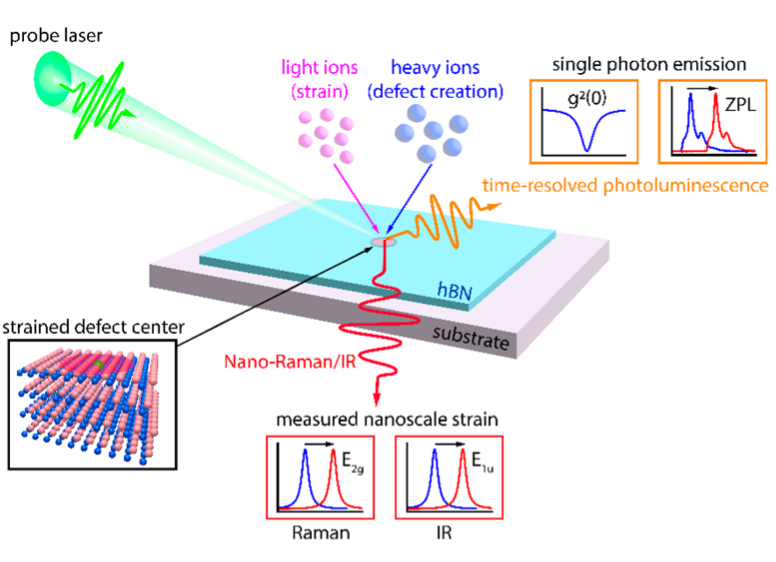
While SPEs have been fabricated in hBN using various methods, the emitters suffer from critical fundamental issues that hinder their use in sensing and networking. As a result, to date there has been no demonstration of a single, scalable process that is able to vary and control the type of defects formed during fabrication. We hypothesize that nanoscale strain and strain gradients could be at the heart of the inhomogenous defect distributions in hBN. Studying these strains and their relations to color center characteristics might therefore hold the key to a fundamentally new level of functionality of solid-state SPEs in 2D materials. This seed project aims at studying and controlling these nanoscale strains using a variety of nanooptical scanning tools and plasma-based fabrication techniques (Fig. 1).

